Scalable production of nano- and microstructures

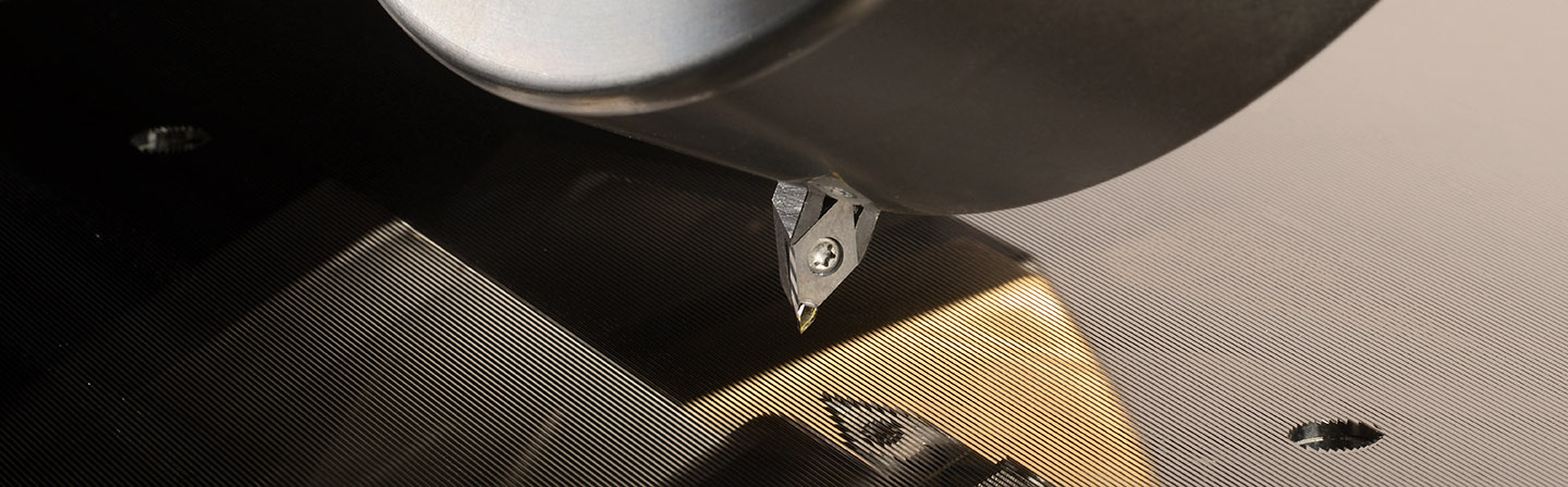
Micro- and nanostructures are used in numerous products: from classic consumer products such as smartphones or monitors, to lighting components in automobiles or for interior design, to medical applications in which, for example, the aim is to promote, diagnose or prevent targeted cell growth.

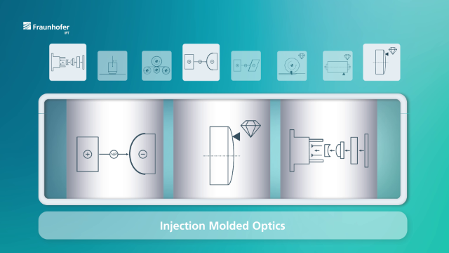
Fraunhofer IPT researches and develops technologies for the manufacture and processing of precision components and has been working on mastering and replication processes for the efficient production of micro- and nanostructures since the 1980s.

Targeted functionalization opens up new applications in medicine, biotechnology and optics

Micro- and nanostructured surfaces, provided with targeted functionalization, can improve efficiency and resource consumption in a wide range of applications. Further developments in materials research and production technology also support numerous new fields of application for micro- and nanostructured surfaces, for example in medicine, biotechnology or for optical components.

Manufacturing miniaturized structures of small and large surfaces requires a large amount of know-how in different disciplines of production engineering and highly complex manufacturing processes. Structures from a few micrometers to a nanometer range can be produced and multiplied in stable replication processes.

Latest technology and process combinations for the automated fabrication of micro- and nanostructures

To this end, Fraunhofer IPT uses the latest machine and software technology to further develop all tasks along various process chains – from tool design to the design and simulation of manufacturing processes to the production of prototypes.

Produce micro- and nanostructures in large quantities or over a large area at low cost

We create the prerequisites for the production of structured component surfaces for a wide variety of application fields. We can manufacture functional microstructures down to the nanometer range from various materials with a variety of production technologies in a cost-optimized manner.


Mastering for high-precision molding tools

We use laser beams and diamond to ablate component surfaces so that the master for your molding tool later delivers highly precise results.

Molding and duplicating microstructures

From a wide variety of molding processes that we master and develop further at the Fraunhofer IPT, we select the right solution for your product.

Our technological know-how around micro- and nanostructures

Production and mastering – structuring processes with light and diamond

Whether in machining, additive manufacturing, or laser ablation processes, the production of micro- and nanostructures requires the highest degree of accuracy and precision.

Optical structures down to just below one micrometer can be produced in machining with monocrystalline diamond as the cutting material. Accessibility for the tool tip is usually the only limiting property here. In 2-photon lithography, an additive process for structures in the nanometer range, only the writing speed sets economic limits. Laser structuring can be used to provide particularly large areas with deeper structures at comparatively low cost. In all these processing methods, however, the requirements for accuracy and precision extend not only to the manufacturing technology used, but also to the upstream and downstream processes.

At Fraunhofer IPT, we bundle competencies across a wide range of production technologies so that all manufacturing stages can be reliably and fully tested. This enables us to develop complete process chains for the manufacture of a wide variety of products with different requirement profiles and bring them to industrial maturity. Examples from this product spectrum include retroreflectors, microlens arrays or aesthetic natural patterns for molded plastic surfaces.

Privacy warning

With the click on the play button an external video from www.youtube.com is loaded and started. Your data is possible transferred and stored to third party. Do not start the video if you disagree. Find more about the youtube privacy statement under the following link: https://policies.google.com/privacy

Laser ablation, planing, grinding, fly-cutting, embossing or lithography: Microstructured components can be manufactured using various processes. With our comprehensive process know-how, we put together the best process chain for each individual application in order to manufacture high-quality components economically.

Highly accurate and flexible for different applications

Depending on the requirements of the material and the subsequent application, the appropriate structuring process must be selected. At Fraunhofer IPT, we work with different technologies that have one thing in common: the highest precision for the requirement profile.


Precision machining

We have been researching machining with diamond tools for more than 30 years with an extensive range of machinery, from which we draw the expertise for a wide range of products.

Lithography

Two-photon polymerization, also known as 2-photon lithography, is an additive process for true 3D printing of photoresists with various optical and chemical properties and structure depths of less than 100 nanometers. A well-known field of application is, for example, the production of tool masters for molding biomaterials for cell cultivation.

Laser structuring

Laser structuring can be used to provide large, even complexly shaped surfaces with structures ranging from several hundred micrometers to the nanometer range, almost independently of the material used.

Galvanic help for microstructuring

Demanding geometries that cannot be produced conventionally by diamond turning or mask lithography can be manufactured galvanically.

Continuous and discontinuous methods for impression taking of micro- and nanostructures

It is only through replication techniques that it is possible to manufacture many products at a marketable price. That is why numerous process chains today rely on these methods for replication.

Fraunhofer IPT not only continues to develop the discontinuous processes of glass forming and injection molding as well as continuous roll-to-roll processes, but is also involved in electroforming for the true-to-shape replication of structures down to the nanometer range. Added to this are multi-step embossing processes to combine small structures on large surfaces.

Our range of services here includes the development of tools and processes for mass production, for example for Fresnel optics, for micro-lens arrays (MLA) made of glass and plastic or for flexible diffuser or antimicrobial protective films, as well as the manufacture of tools for mastering processes, which often enable the cost-reducing upscaling of production in the first place.

Molding, forming, injection molding – replication processes for large quantities

In particular, optical components for the consumer sector or consumables for medical or pharmaceutical applications provide good examples of why it is becoming increasingly important to make even high-precision components available in large quantities. Replication processes open up opportunities here to make new and high-demand products available to the market quickly and cost-effectively.


Molding from roll to roll

By molding via roll-to-roll processes, large-area microstructures and nanostructures can be reproduced on plastic film at low cost.

Injection molding of plastic components

Injection molding is a cost-effective way to produce plastic optics or microfluidic disks with high dimensional accuracy.

Blank pressing of glass components

Non-isothermal blank pressing can be used to produce microstructured surfaces from glass at low cost.

Precision glass molding

The production of wafers by precision molding is used to make micro- and nanostructured glass components available quickly and in large quantities at low cost.

Step-and-repeat hot stamping

In a multi-step hot stamping process, microstructures with optical properties can be introduced into polymer surfaces over large areas and at low cost.

Projects in the field of micro- and nanostructuring

Publicly funded projects enable us to break new technological ground. With a selection of our current projects, you can get an impression of the direction in which we are heading.


Tamper-proof fingerprint sensor

The goal in the "KomFiDis" project is the precise and cost-effective replication of optical structures for the sensor's OLED microdisplay.

Intelligent light management

The aim of the project is to develop a process chain for the production of low-reflection nanostructured optical components that are used in infrared sensors for energy-saving light management.

Anti-reflective structures for point gas sensors

For a compact and robust point gas sensor that can detect methane gas, we replicate infrared optics with anti-reflective structures using precision molding.


Head-up displays for large vehicles

High-performance plastic optics can help increase the field of view of head-up displays without the systems taking up further space in the vehicle's cockpit.