 Fraunhofer Institute for Production Technology IPT
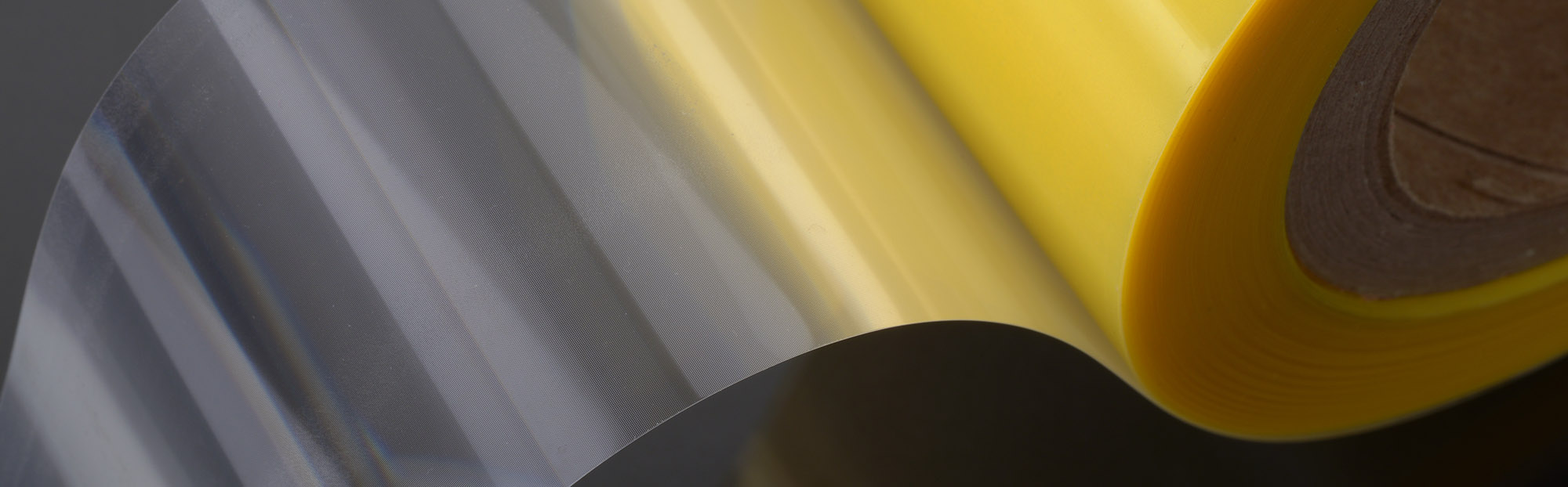

Lightweight components, mobile devices and displays require highly integrated, functional elements in order to meet the need for increasingly compact, flat and more powerful technological solutions. Films with a thickness of a few tenths of a millimeter offer optimal conditions for representing a broad spectrum of optoelectronic or microfluidic elements and for replacing conventional components. Printed electronics, optical films, lab-on-a-chip systems and biomimetic nanostructures can be produced in continuous roll-to-roll processes. Their production is scalable and cost-efficient thanks to digital manufacturing approaches.
Areas of application of multifunctional films
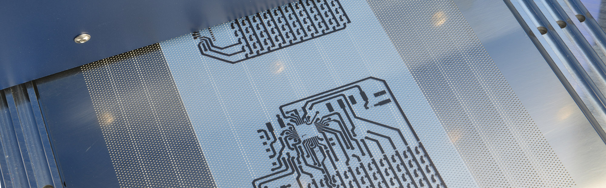
Microlenses, produced on large surfaces, can be used to collimate light for optical sensors, to remove the glare of light guides or to create defined laser beam characteristics – all in the form of an optical film. Also, flexible conducting paths printed on transparent film are feasible. Simple, flexible circuits can be achieved in combination with conventional SMD components. Furthermore, micro- and nanostructures can be embossed into large surfaces with high precision – an interesting application for medicine and biotechnology as well as for inexpensively producing holographic safety labels.
From product development to production system development
The Fraunhofer IPT supports its partners in the fields of industry and research throughout the entire process, from conducting feasibility studies, producing prototypes to small series production. As an institute for production technology, we also provide production system development in addition to product development. Together with our R&D partners, our employees produce customised system solutions as well as machine prototypes, including commissioning and process optimization.
Our service
- Optical films: large-surface microlenses for collimation or defined shaping of light
- Films with microfluidic structures: lab-on-a-chip systems
- Printed electronics: printed, flexible conducting paths and simple, hybrid circuits
- Micro and nanostructure films: applications in biotechnology, medicine and security