 Fraunhofer Institute for Production Technology IPT
LASER World of PHOTONICS
Precision at Scale: Fraunhofer IPT Showcases Industrial Optics Manufacturing Technologies at LASER World of PHOTONICS
At this year’s LASER World of PHOTONICS in Munich, Fraunhofer Institute for Production Technology IPT will present cutting-edge manufacturing technologies for next-generation optics production. Visitors will find the team in Hall B1, Booth 231. The exhibits are geared toward companies looking to manufacture high-precision glass components efficiently, scale micro- and nanostructures, or perform inline quality control of optical parts.
Fraunhofer IPT will spotlight three core technologies addressing key challenges in industrial optics manufacturing: precision glass molding, scalable microstructuring, and non-destructive inspection of miniaturized components.
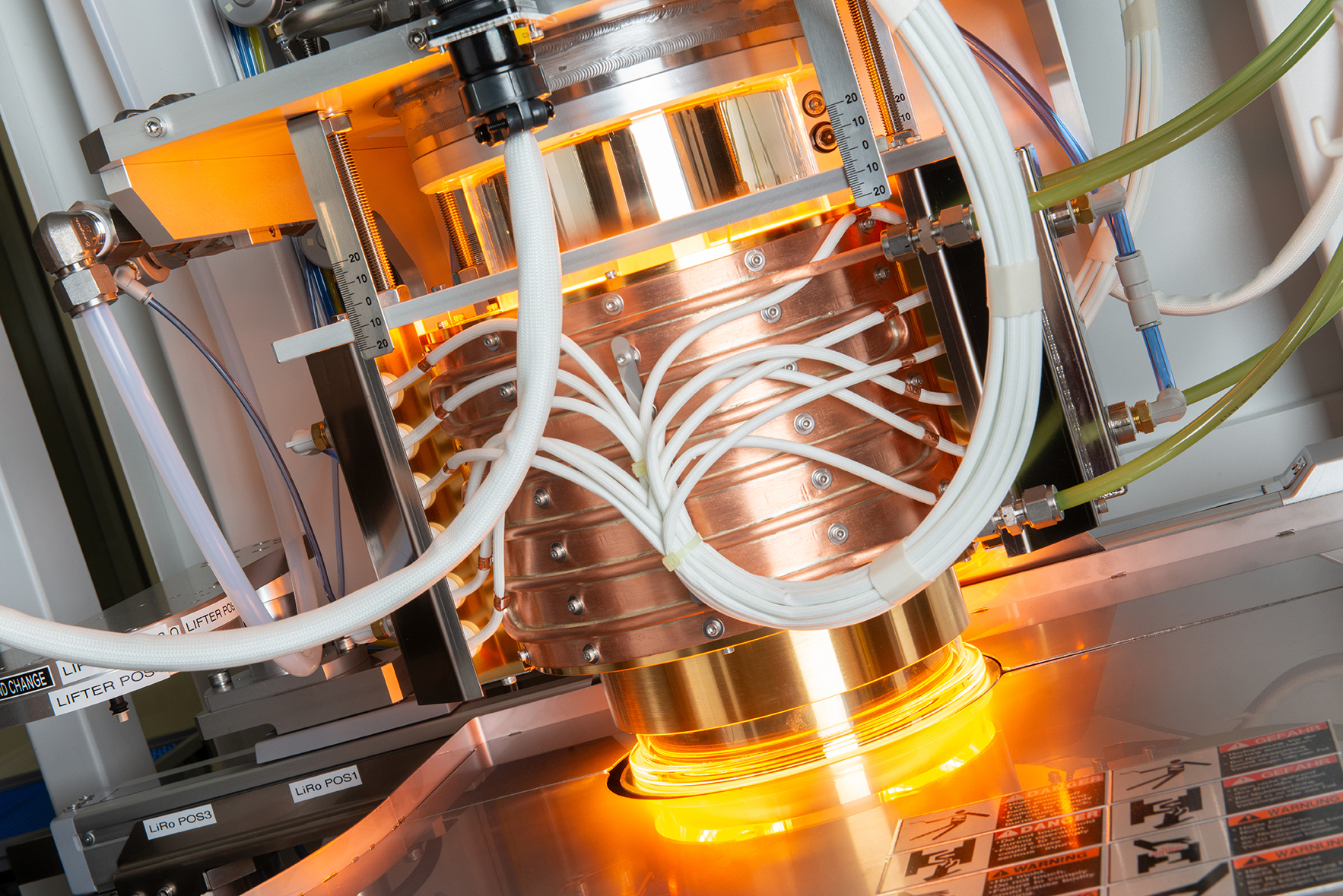
Glass Molding: Complex Geometries, Mass-Produced with Consistency
At the booth, the team will display a range of optical glass components manufactured through replicative molding—including micro-optics, lens arrays, and structured substrates. The associated molds are produced in-house using ultra-precision machining with sub-micron accuracy. The goal: to make complex geometries with tight tolerances scalable for industrial production—efficiently, reproducibly, and in series. This opens new opportunities for companies in the semiconductor, medical, and aerospace sectors to create miniaturized parts that previously required costly subtractive manufacturing.
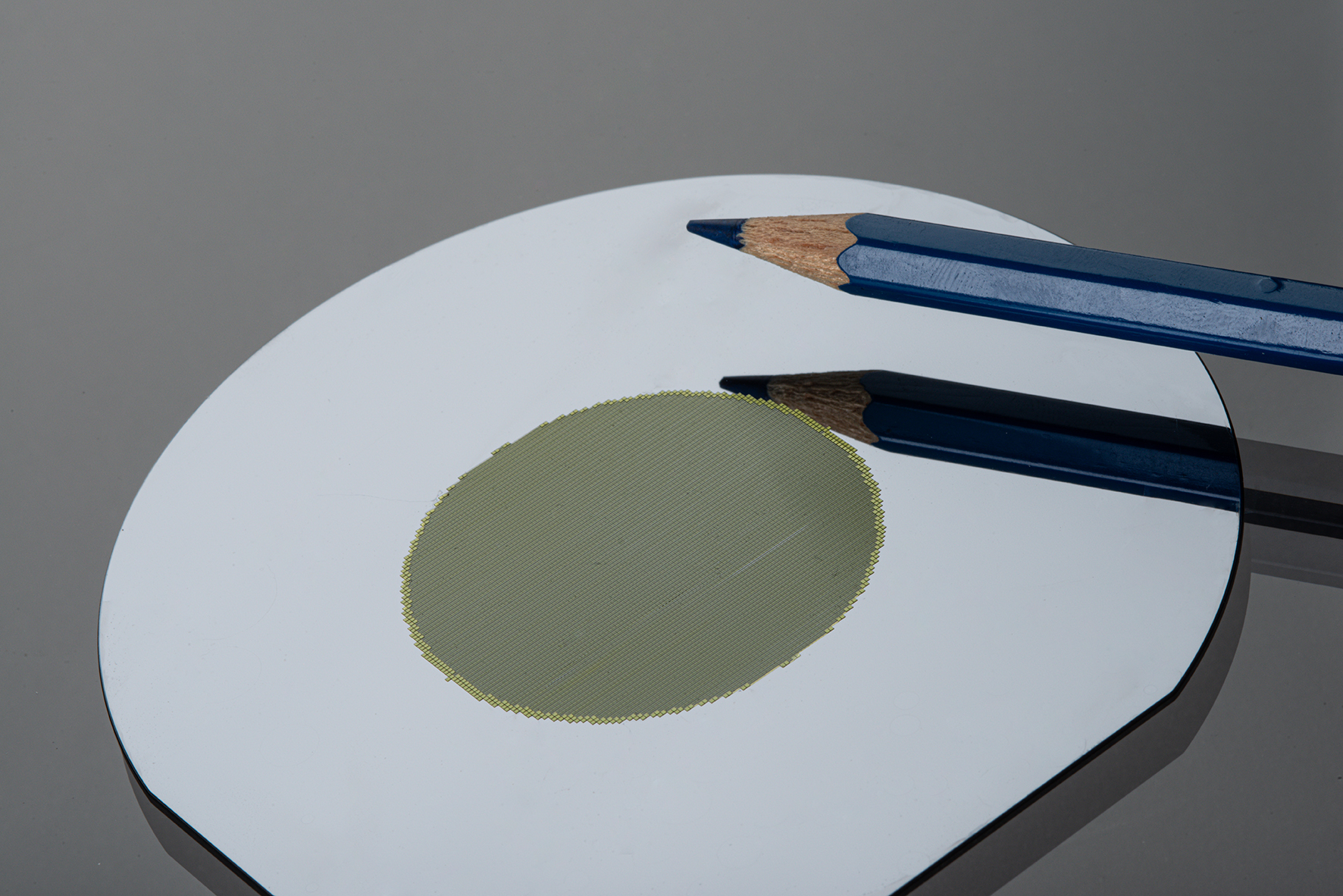
Micro- and Nanostructuring: Scalable by Design
The institute will also showcase the complete process chain for large-area micro- and nanostructures, from the master template to the replicated substrate. Central to this approach is a technique that assembles smaller structural units into a seamless, large-area mold. This architecture shortens processing time, improves reproducibility, and reduces costs. It’s particularly well-suited for optical surfaces, sensors, and functional coatings—applications where structure quality and scale have traditionally been difficult to reconcile.
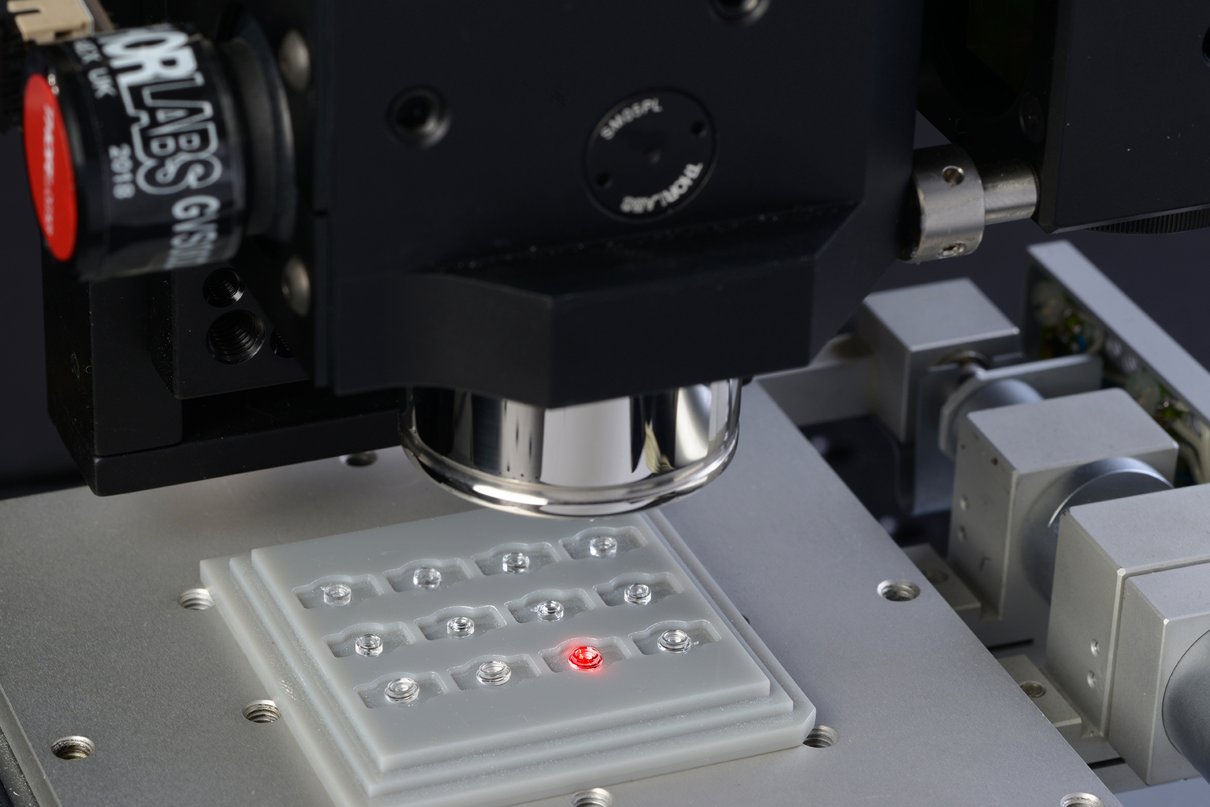
Metrology: Non-Destructive Testing for Miniaturized Optics
A live demo of Fraunhofer IPT’s OCT (Optical Coherence Tomography) system will show how plastic and glass micro-optics can be inspected contact-free—providing cross-sectional views, 3D geometry data, and precise layer thickness measurements. The system detects internal defects, measures complex multi-material shapes, and enables inline quality control that cuts development time and minimizes scrap. The technology is especially valuable for manufacturers of microlenses, lens arrays, or tightly specified optical assemblies.
From Research to Production
Each exhibit is rooted in research projects with a clear industrial focus: more precise processes, robust manufacturing methods, and shorter cycle times. The ultimate aim: to bridge the gap between the lab and the factory floor—making breakthrough technologies production-ready.